
第1页 / 共77页
试读已结束,还剩76页,您可下载完整版后进行离线阅读
THE END
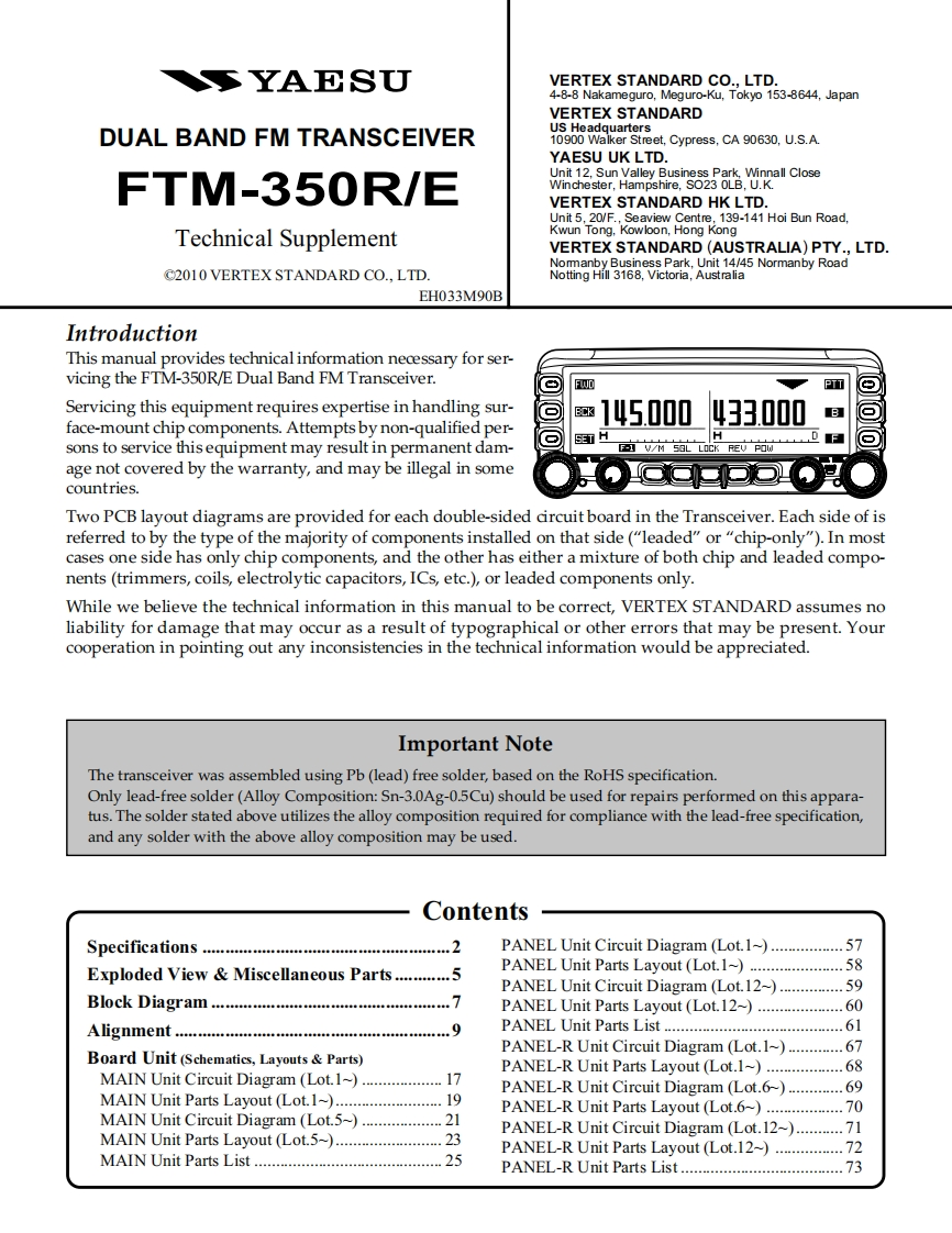
NSYAESUVERTEX STANDARD CO.,LTD.4-8-8 Nakameguro,Meguro-Ku,Tokyo 153-8644,JapanVERTEX STANDARDDUAL BAND FM TRANSCEIVERUS Headquarters10900 Walker Street,Cypress,CA 90630.U.S.A.YAESU UK LTD.FTM-350R/EW NampreCloseVERTEX STANDARD HK LTD.Unit 5,20/F.,Seaview Centre,139-141 Hoi Bun Road,Technical SupplementKwun Tong,Kowloon,Hong KongVERTEX STANDARD(AUSTRALIA)PTY.,LTD.Nomanby Business Park,Unit 14/45 Normanby Road2010 VERTEX STANDARD CO.,LTD.Notting Hill 3168,Victoria,AustraliaEH033M90BIntroductionThis manual provides technical information necessary for ser-vicing the FTM-350R/E Dual Band FM Transceiver.F吧PTTServicing this equipment requires expertise in handling sur-14500033000face-mount chip components.Attempts by non-qualified per-sons to service thisequipment may result in permanent dam-SET HIV/M SBL LOCK REV POWage not covered by the warranty,and may be illegal in somecountries.Two PCB layout diagrams are provided for each double-sided circuit board in the Transceiver.Each side of isreferred to by the type of the majority of components installed on that side("leaded"or"chip-only").In mostcases one side has only chip components,and the other has either a mixture of both chip and leaded compo-nents(trimmers,coils,electrolytic capacitors,ICs,etc.),or leaded components only.While we believe the technical information in this manual to be correct,VERTEX STANDARD assumes noliability for damage that may occur as a result of typographical or other errors that may be present.Yourcooperation in pointing out any inconsistencies in the technical information would be appreciated.Important NoteThe transceiver was assembled using Pb(lead)free solder,based on the RoHS specification.Only lead-free solder (Alloy Composition:Sn-3.0Ag-0.5Cu)should be used for repairs performed on this appara-tus.The solder stated above utilizes the alloy composition required for compliance with the lead-free specification,and any solder with the above alloy composition may be used.ContentsSpecifications2PANEL Unit Circuit Diagram (Lot.1)57Exploded View Miscellaneous Parts............5PANEL Unit Parts Layout (Lot1)58PANEL Unit Circuit Diagram (Lot.12~).............59Block Diagram.9PANEL Unit Parts Layout (Lot.12~)....................60Alignment……9PANEL Unit Parts List61PANEL-R Unit Circuit Diagram (Lot.1~).............67Board Unit (Schematics,Layouts Parts)PANEL-R Unit Parts Layout (Lot.1~).................68MAIN Unit Circuit Diagram (Lot.1~).................17PANEL-R Unit Circuit Diagram (Lot.6~)............69MAIN Unit Parts Layout (Lot1)19PANEL-R Unit Parts Layout (Lot.6~)............70MAIN Unit Circuit Diagram (Lot.5~)................21MAIN Unit Parts Layout (Lot.~)......PANEL-R Unit Circuit Diagram (Lot.12~)...........7123PANEL-R Unit Parts Layout (Lot.12~).............72MAIN Unit Parts List.…25PANEL-R Unit Parts List.3

请登录后查看评论内容