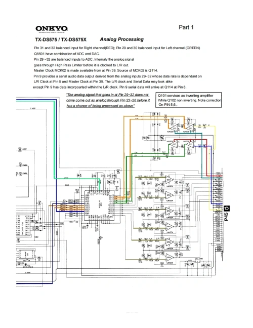
ONKYOPart 1TX-DS575/TX-DS575XAnalog ProcessingPin 31 and 32 balanced input for Right chamel(RED Pin 29 and 30 balanced inout for Left channel (GREEN)C8501 have combinstion of ADC and DAC.Pin 29-32 are balanoed inputs to ADC.Intemaly the aralg signalgoes through High Pass Limiter before it is clocked to LR outaster Clock MCK02sm线available from黄Ph39.Sorc86fMC×0叹sQ114Pin 9 provides a serial audo data ouput derived from the analog inputs 29-32 whose data rate is dependant onUR Cbo atP叫n58 nd Maste白ock at Pi39.The UR dock and Serial Data m时y look a地except Pn9 has data ncorpoarted within the LR dock.Pn9 ris dat情larrive剩Q1i4碳Pin8The anabg stcal mat goes in Pn 29-32 does notQ101 servicis as irering ampifera2酸n9h29tPm22-28ee星While Q102 non inverting.Note comectiorEAha进f地h回PDe5型b2On PN56


请登录后查看评论内容