
第1页 / 共79页
第2页 / 共79页
试读已结束,还剩77页,您可下载完整版后进行离线阅读
THE END
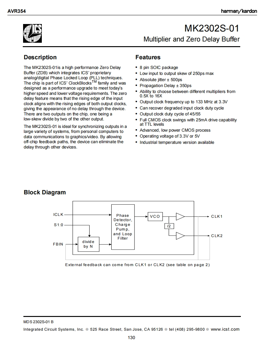
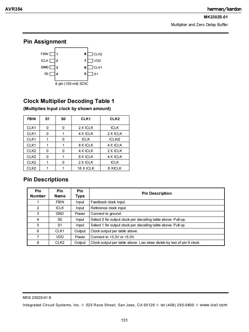
AVR354harman/kardonMK2302S-01Multiplier and Zero Delay BufferDescriptionFeaturesThe MK2302S-01is a high performance Zero Delay·8 pin SOIC packageBuffer(ZDB)which integrates ICS'proprietaryLow input to output skew of 250ps maxanalog/digital Phase Locked Loop (PLL)techniques.The chip is part of ICS'ClockBlocksTM family and was·Absolute jitter:±500psdesigned as a performance upgrade to meet today's·Propagation Delay±350pshigher speed and lower voltage requirements.The zeroAbility to choose between different multipliers from0.5X to 16Xdelay feature means that the rising edge of the inputclock aligns with the rising edges of both output docks.Output clock frequency up to 133 MHz at 3.3Vgiving the appearance of no delay through the device.Can recover degraded input clock duty cycleThere are two outputs on the chip,one being a.Output clock duty cycle of 45/55low-skew divide by two of the other output.Full CMOS clock swings with 25mA drive capabilityThe MK2302S-01 is ideal for synchronizing outputs in aat TTL levelslarge variety of systems,from personal computers toAdvanced,low power CMOS processdata communications to graphics/video.By allowingOperating voltage of 3.3V or 5Voff-chip feedback paths.the device can eliminate theIndustrial temperature version availabledelay through other devices.Block DiagramICLK-PhaseVcoCLK1Detector.S1:0Charge2Pump,and LoopCLK2FilterFBINdivideby NExternal feedback can come from CLK1 or CLK2 (see table on page 2)MDS 2302S-01 BIntegrated Circuit Systems,Inc.525 Race Street,San Jose,CA 95126tel(408)295-9800 www.icst.com130

请登录后查看评论内容