
第1页 / 共121页
试读已结束,还剩120页,您可下载完整版后进行离线阅读
THE END
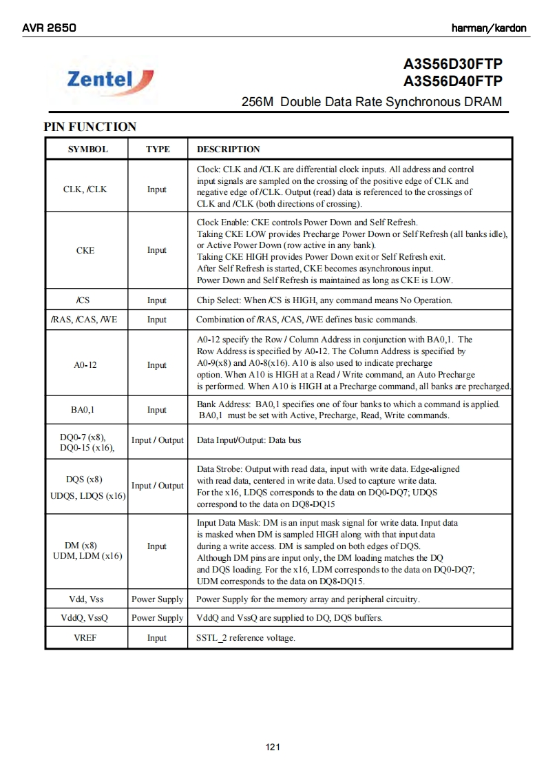
AVR 2650harman/kardonA3S56D30FTPZentelA3S56D40FTP256M Double Data Rate Synchronous DRAMPIN FUNCTIONSYMBOLTYPEDESCRIPTIONClock:CLK and /CLK are differential clock inputs.All address and controlinput signals are sampled on the crossing of the positive edge of CLK andCLK,/CLKInputnegative edge of/CLK.Output(read)data is referenced to the crossings ofCLK and /CLK (both directions of crossing).Clock Enable:CKE controls Power Down and Self Refresh.Taking CKE LOW provides Precharge Power Down or SelfRefresh (all banks idle),CKEInputor Active Power Down(row active in any bank).Taking CKE HIGH provides Power Down exit or Self Refresh exit.After Self Refresh is started,CKE becomes asynchronous input.Power Down and Self Refresh is maintained as long as CKE is LOW./CSInputChip Select:When/CS is HIGH,any command means No Operation./RAS,/CAS,/WEInputCombination of/RAS,/CAS,/WE defines basic commands.A0-12 specify the Row/Column Address in conjunction with BA0,1.TheRow Address is specified by A0-12.The Column Address is specified byA0-12InputA0-9(x8)and A0-8(x16).A10 is also used to indicate prechargeoption.When A10 is HIGH at a Read/Write command,an Auto Prechargeis performed.When A10 is HIGH at a Precharge command,all banks are precharged.BA0,1InputBank Address:BA0,I specifies one of four banks to which a command is applied.BA0,1 must be set with Active,Precharge,Read,Write commands.DQ0-7(x8),Input/OutputData Input/Output:Data busDQ0-15(x16),Data Strobe:Output with read data,input with write data.Edge-alignedDQS (x8)Input/Outputwith read data,centered in write data.Used to capture write data.UDOS,LDOS (x16)For the x16,LDQS corresponds to the data on DQ0-DQ7;UDQScorrespond to the data on DQ8-DQ15Input Data Mask:DM is an input mask signal for write data.Input datais masked when DM is sampled HIGH along with that input dataDM (x8)Inputduring a write access.DM is sampled on both edges of DQS.UDM,LDM(x16)Although DM pins are input only,the DM loading matches the DQand DQS loading For the x16,LDM corresponds to the data on DQ0-DQ7;UDM corresponds to the data on DQ8-DQ15.Vdd,VssPower SupplyPower Supply for the memory array and peripheral circuitry.VddQ,VssQPower SupplyVddQ and VssQ are supplied to DQ,DQS buffers.VREFInputSSTL_2 reference voltage.121

请登录后查看评论内容